Demo Lab.
Engis Japan provides
Total Lapping / Polishing Solution
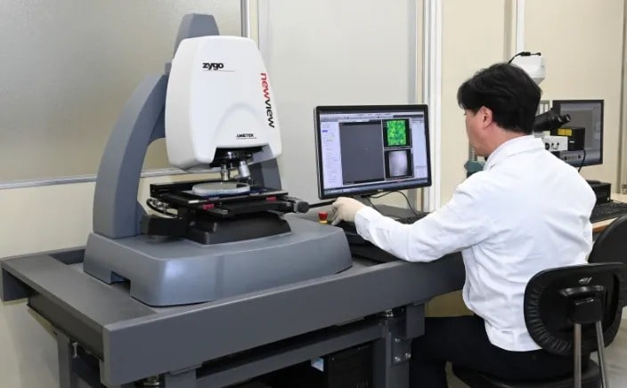
Providing
Comprehensive Solutions
Our demo lab, which is the core of our company, is working every day to meet a wide variety of needs.
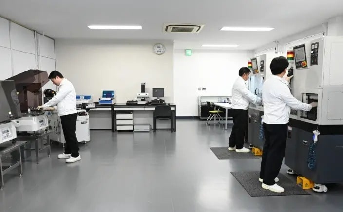
Process
Demonstration
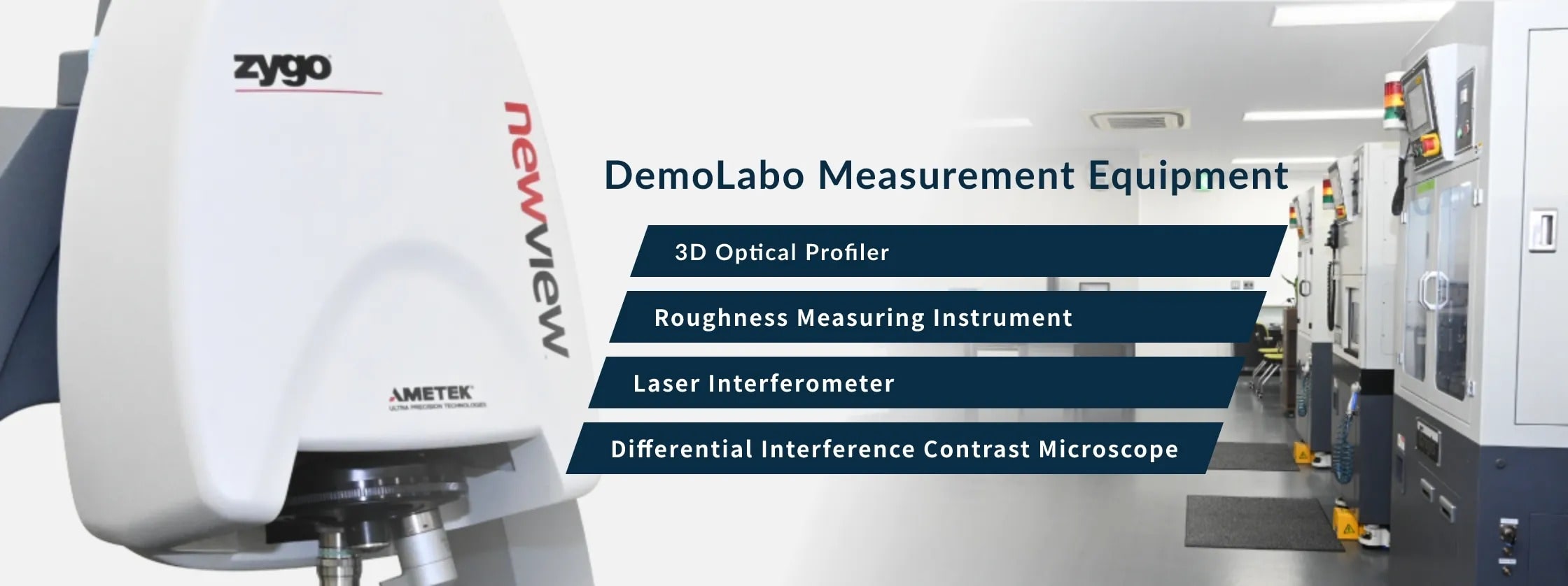
We are fully equipped with measuring equipment so that we can instantly evaluate after polishing, so we can immediately find the optimum processing conditions that meet the customer's request.
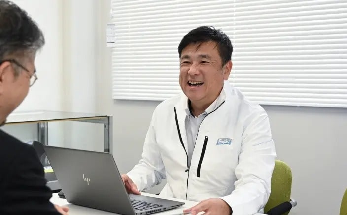
Support by
Experienced Staff
From system consideration to post-delivery, we will propose the optimum system and process according to the customer's purpose of use and installation environment.
- Case.01Diamond Lapping System
- Case.02Compound Semiconductor Wafer Bonding - Grinding - CMP Process
- Case.03SiC Wafer Thinning Process
-
Case.04Hydraulic Pump -
Piston Pump Parts
Case.01
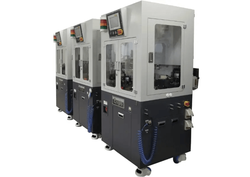
Diamond Lapping System
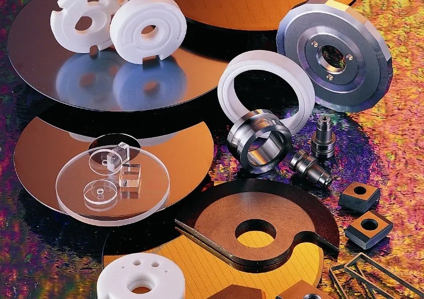
The facing mechanism, which is indispensable for calling it an ultra-precision lapping machine, forms a highly accurate flat shape over the entire lapping plate. A diamond lapping system maintains absolute flatness accuracy and a stable mirror surface is used in a wide range of fields for surface processing such as optical flat, molds and machine parts that require high-precision flatness and mirror surface.
Process
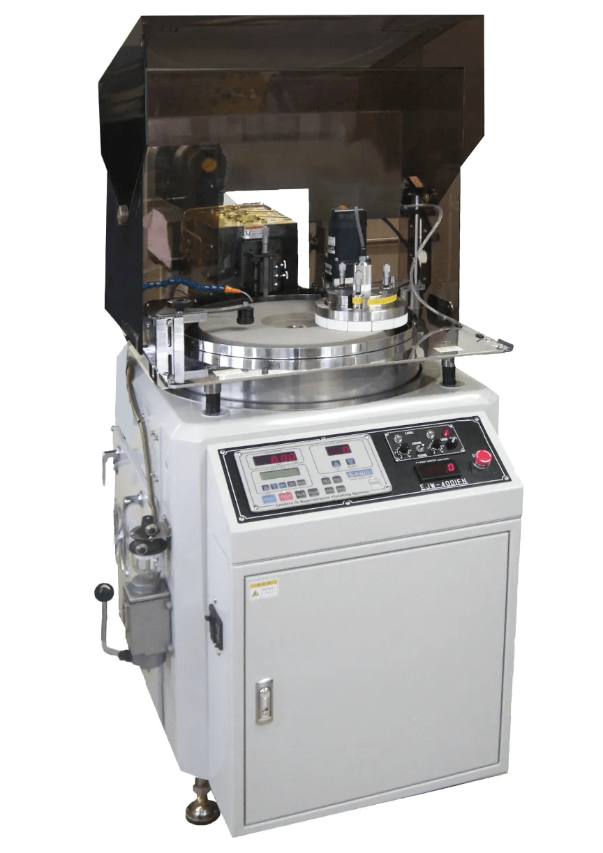
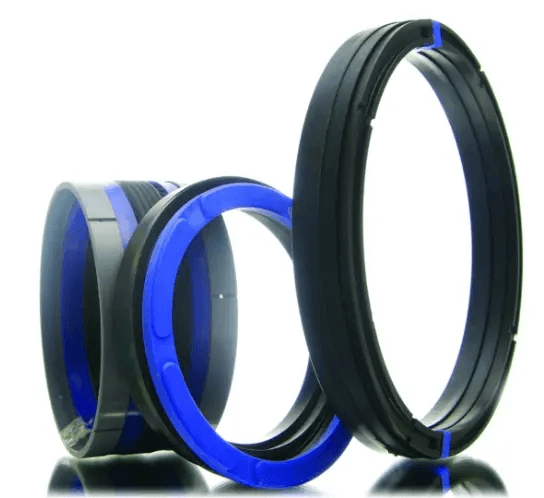
Mechanical Seal Flat Lapping
- Work Piece : Mechanical Seal Ring
- Material : Carbon
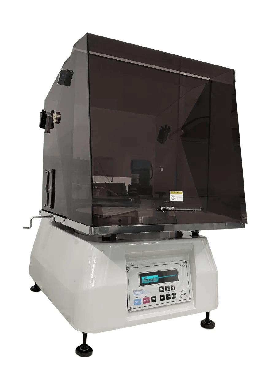
- Lapping Machine : EJW-400IFN
- Lap Plate : HY Copper
- Slurry : 3um Diamond Slurry
- Cycle Time : 10mins
- Flatness < 0.5um
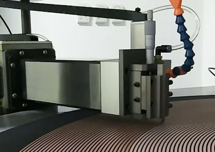
Molding Die Flat Lapping / Mirror Finishing
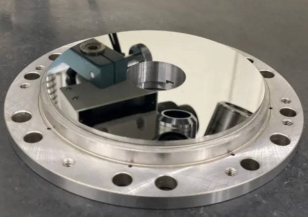
- Work Piece : Optical Disc Mold
- Material : SUS420
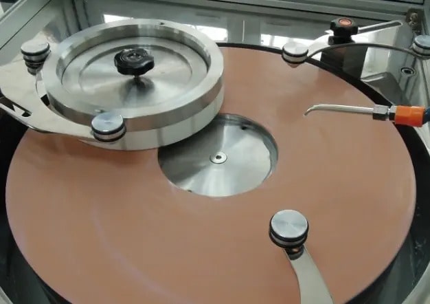
- Lapping Machine : EJ-380IN
- Lap Plate : HY Copper >>> 530N Pad
- Slurry : Diamond 3um >>> HCL-XL
- Cycle Time : Lapping 20mins / Polish 5mins
- Flatness : < 0.3um / Roughness : < 1nmRa
Case.02
Compound Semiconductor Wafer
Bonding - Grinding - CMP Process
Compound semiconductors such as InP/GaAs/GaSb are used in high-frequency devices, light-emitting devices, and power devices.
In the thinning polish process, which is the pre-process of the chip process, wafer bonding, grinding, and polishing processes are performed to finish wafers with thickness of 100um or less with free of scratches, cracks, and stress.
Process
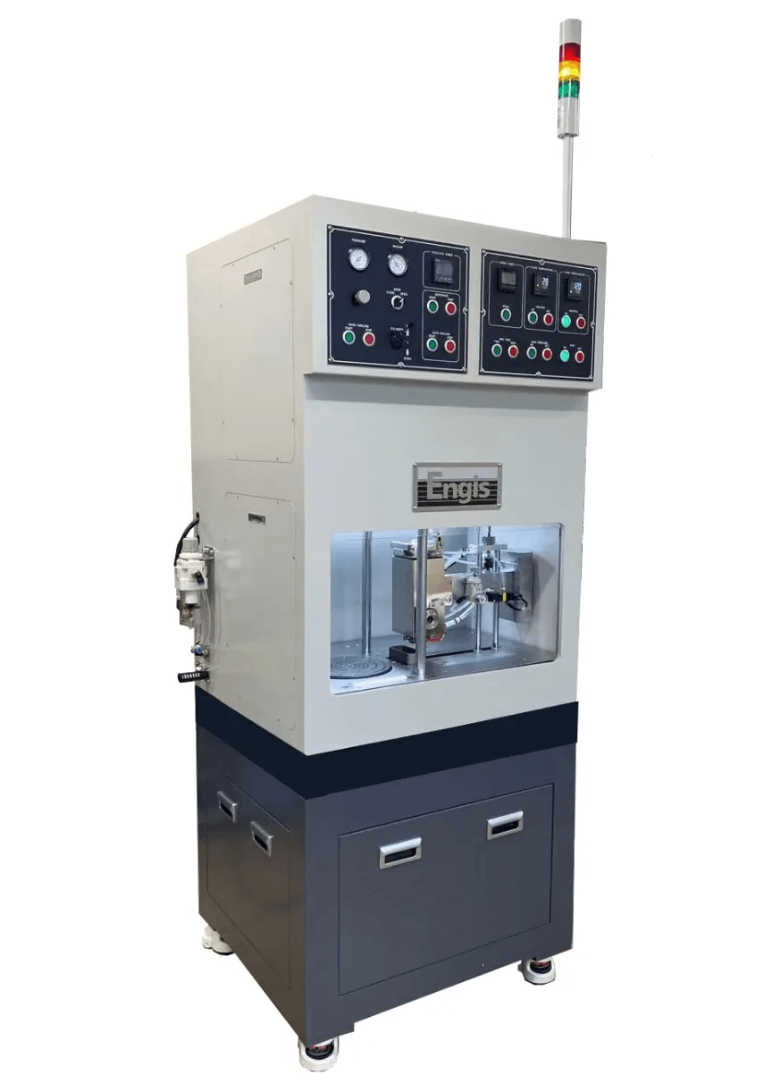
InP Thinning Process
1. Bonding Process
- Semi-Auto Bonding Machine
MODEL : EBM-200HCD - Bonding Process
Mounting wafer on ceramics or glass plate - Achievement
Wax thickness variation 1~3um
Variation (TTV) < 1um
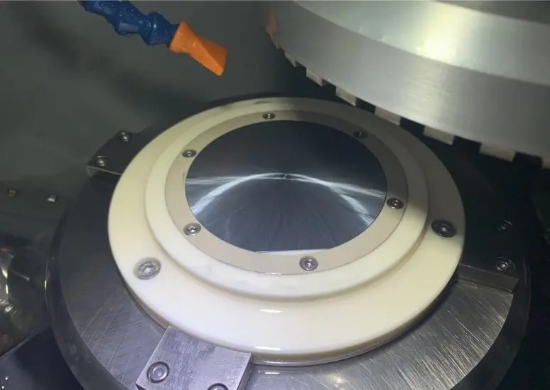
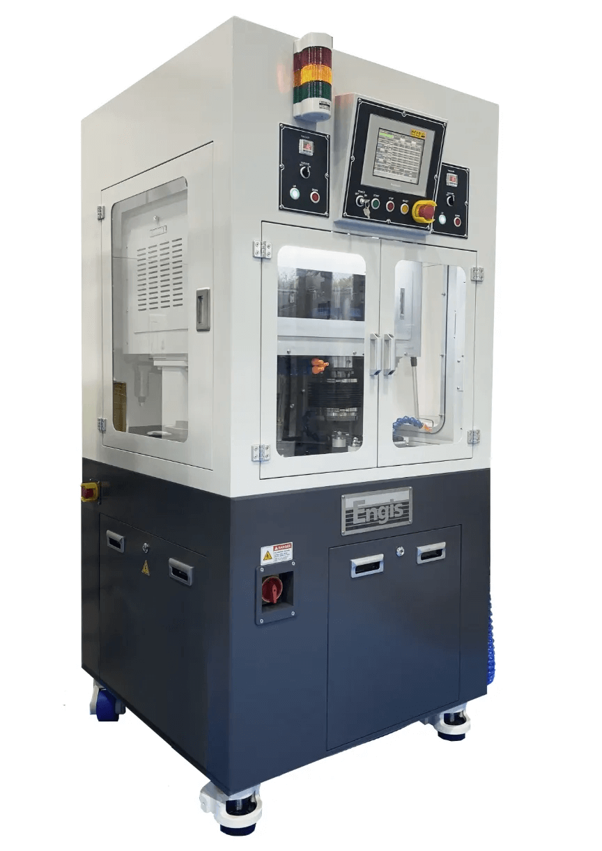
2. Grinding Process
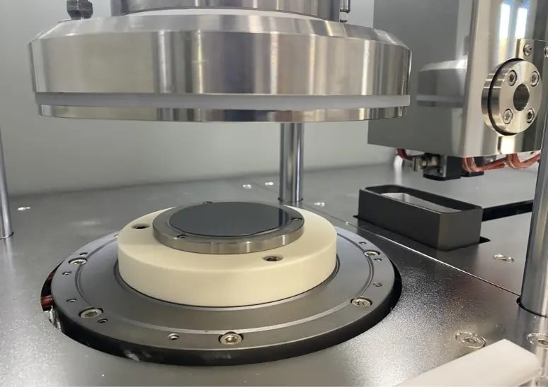
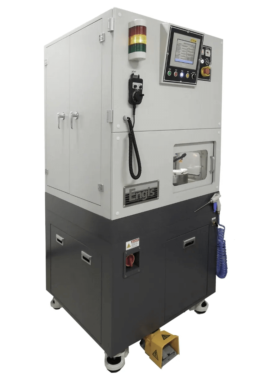
- Vertical Grinding Machine
MODEL : HVG-250ADM - Grinding Process
Controlling wafer thickness and variation, improve roughness - Achievement
Roughness < 10nmRa
Thickness : 120um
Thickness Variation TTV < 1um
3. CMP Process
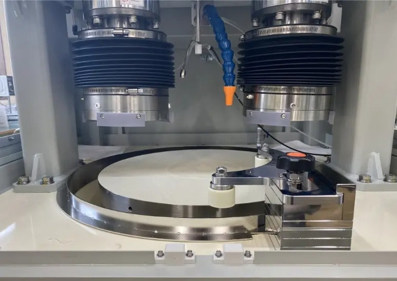
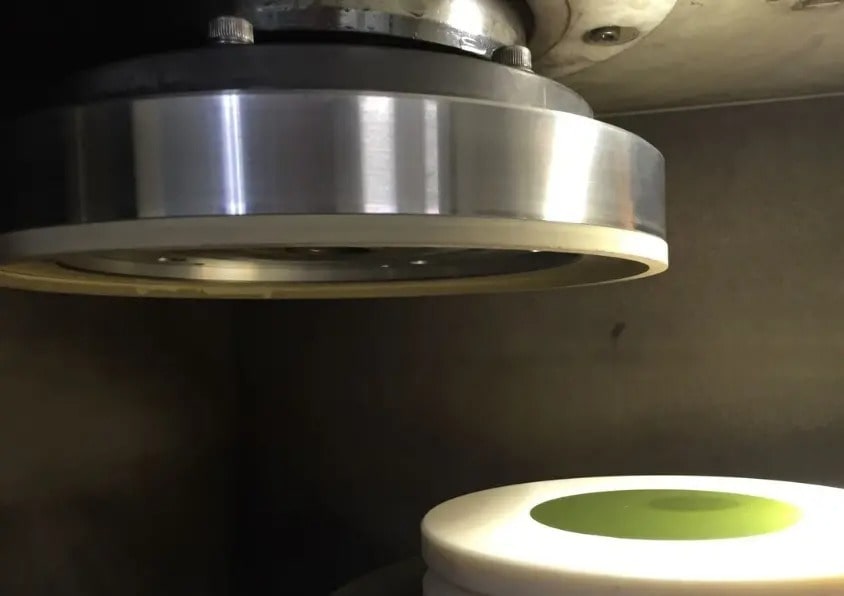
- CMP Machine
MODEL : EJW-460I-2ALD-D - Removing surface damage and stress remaining from grinding by CMP process
- Achievement
Roughness < 0.5nmRa
Stress free
Case.03
Silicon carbide thin wall grinding
In recent years, in order to realize energy saving and low carbonization, it is essential to improve the efficiency of power conversion, and commercialization is accelerating. A high-performance motor is mounted on the grinding wheel shaft of the new 2-axis grinder EVG-300DSO, which is expected to further improve the quality and efficiency of polishing processing technology for SiC power semiconductor devices, which is a representative of such devices. We introduce examples of the latest wafer polishing process technology using grinding processing and polishing equipment.
Process
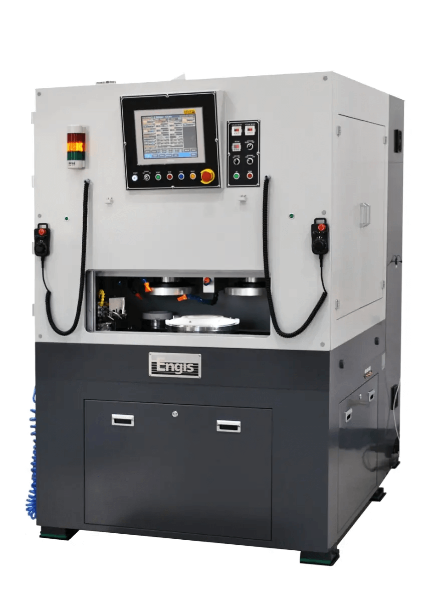
SiC Wafer Thinning Process
1. Grinding Process
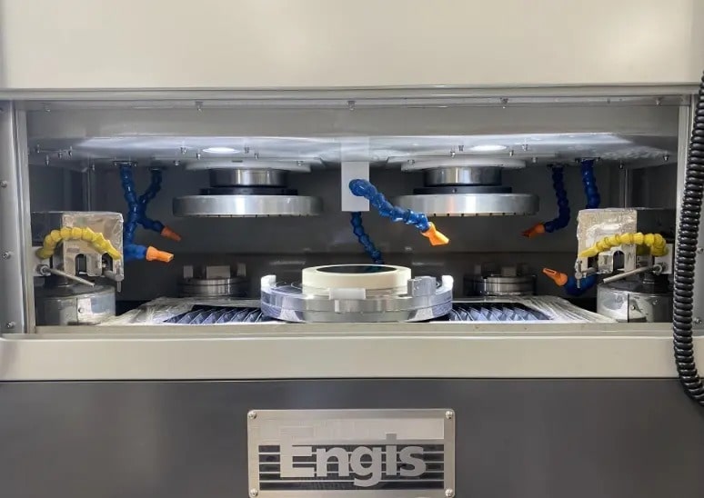
- 2-spindles Vertical Grinding Machine
MODEL : HVG-300DSO - Grinding
Controlling wafer thickness and variation, improve surface roughness - Achievement
Roughness < 1nmRa
Thickness : 120um
Thickness variation (TTV) < 1um
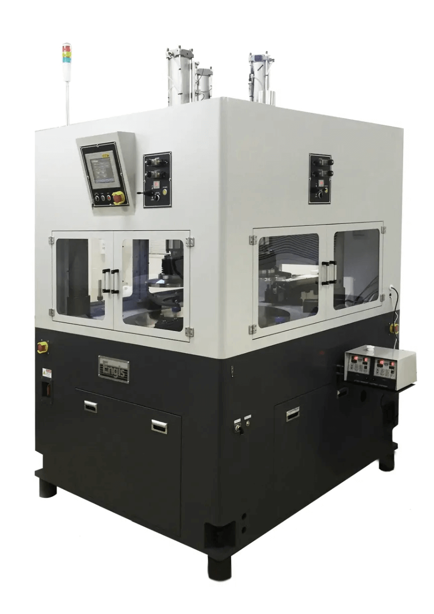
2. Polishing Process
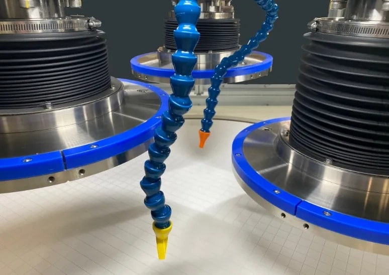
- 3-stations Polishing Machine
MODEL : EJW-910I-3ALD-D - CMP Process
Removing surface damage and stress remaining from grinding by CMP process using Diamond or CMP slurry. - Achievement
Surface roughness < 0.5nmRa
Stress free
Case.04
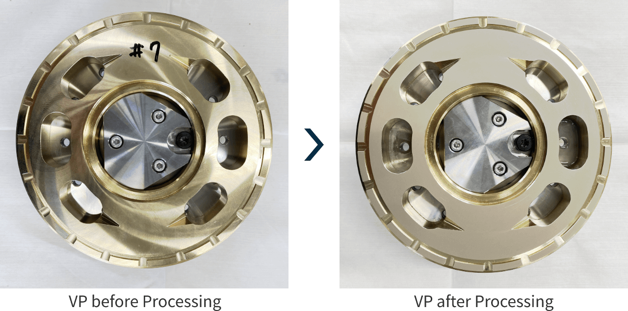
Hydraulic Pump - Piston Pump Parts
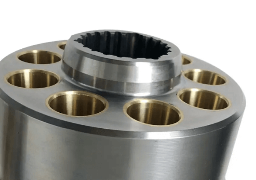
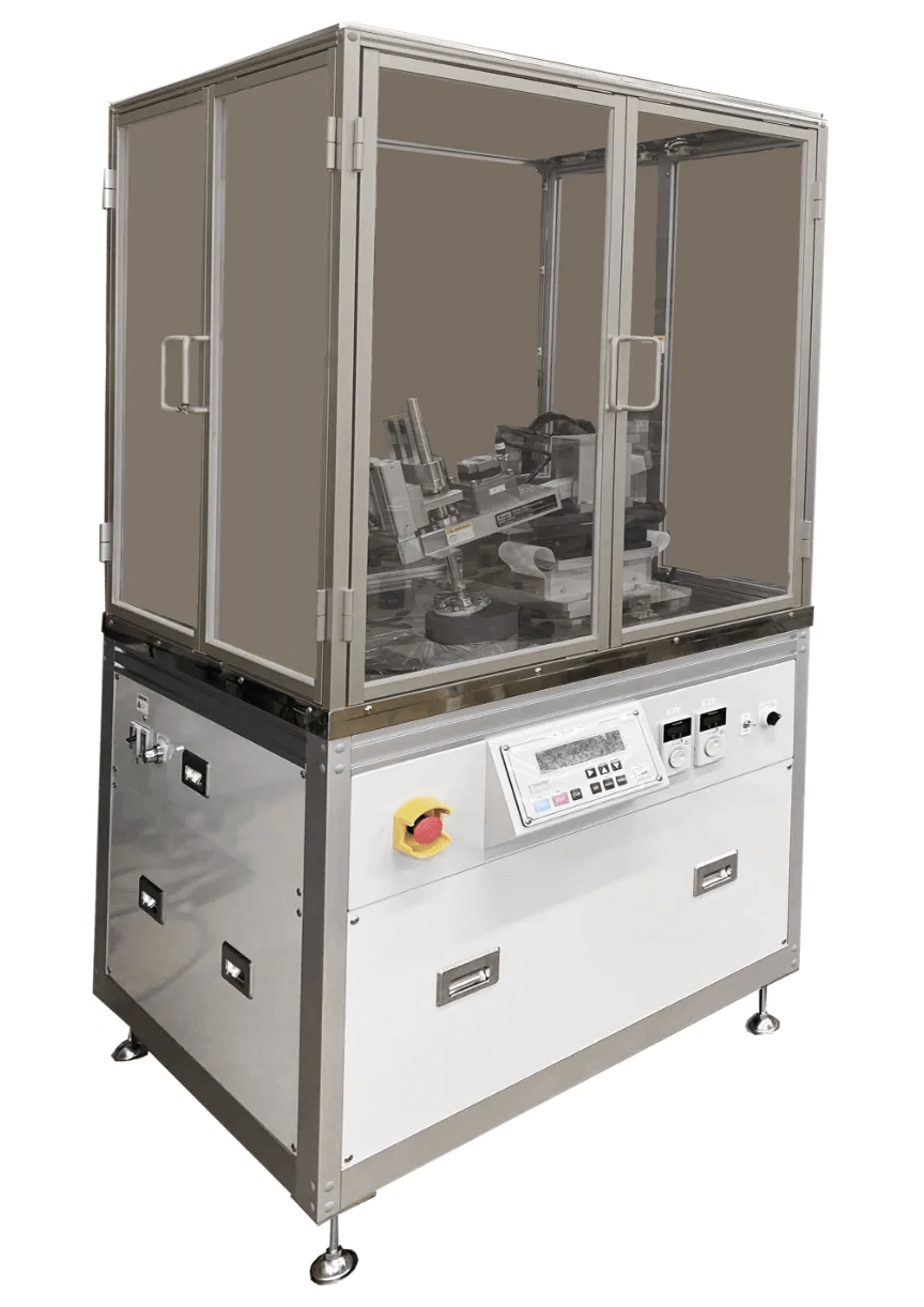
Utilizing our extensive experience and knowledge of lapping technology that we have cultivated over many years, we have successfully developed our own spherical polishing machine "EJ-380ISR-TETRA" (Tetra), which mechanizes the rubbing work of hydraulic pump parts. By using this innovative spherical surface polishing device Tetra, it is possible to mechanize the "rubbing work" used to polish the mating surfaces of the cylinder block and valve plate, which are the heart of the swash plate type axial piston pump.
Process
Piston Pump Lapping
1. Lapping Process
- Spherical Lapping Machine
MODEL:EJ-380ISR-TETRA - Master Lap Process
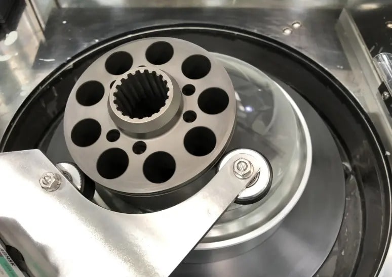
Lapping valve plate and master plate together to transfer the exact shape of the master plate to the valve plate. - Achievement
Cycle Time : 4-6 mins
Roughness < 0.2umRa
2. Pair Lap Process
- Spherical Lapping Machine
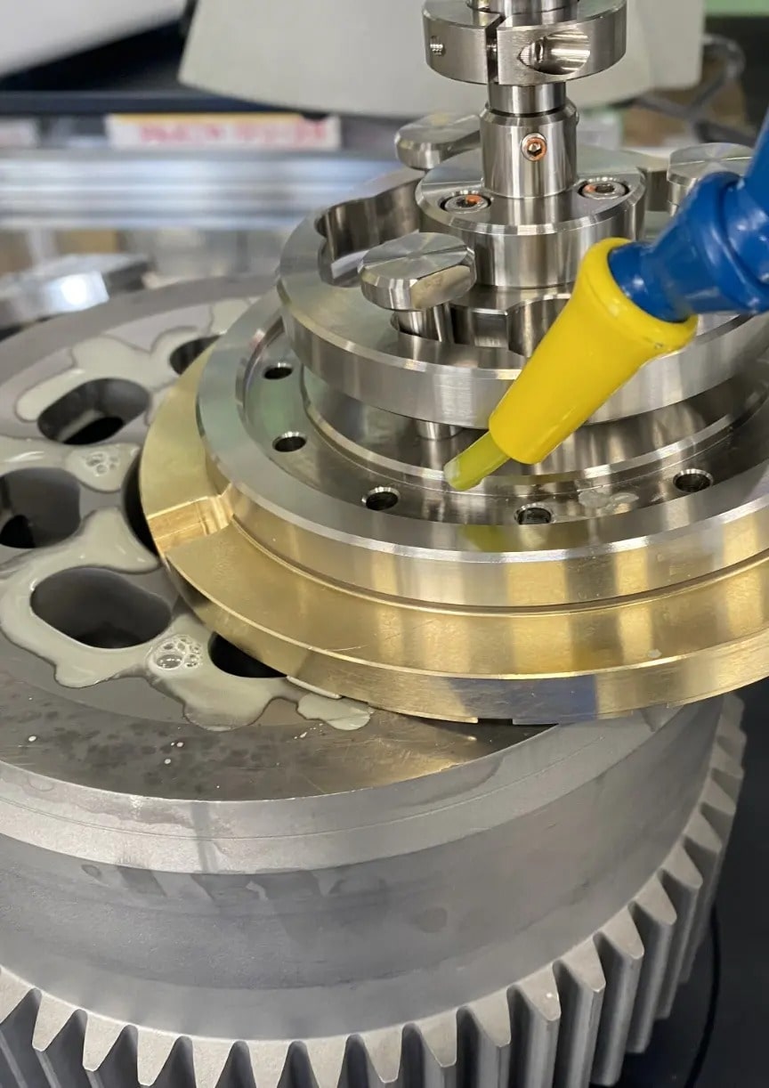
MODEL:EJ-380ISR-TETRA - Pair Lap Process
Lapping valve plate and cylinder block together to improve contact ratio - Achievement
Cycle Time : 4-6 mins
Roughness < 0.2umRa
Contact Ratio > 99.8%
